Intel Introduces Gaudi 3 AI Accelerator: Going Bigger and Aiming Higher In AI Market
by Ryan Smith on April 9, 2024 11:35 AM EST- Posted in
- GPUs
- Intel
- Accelerator
- AI
- HBM2E
- Habana
- Gaudi
- Gaudi 3
- Intel Vision 2024
Intel this morning is kicking off the second day of their Vision 2024 conference, the company’s annual closed-door business and customer-focused get-together. While Vision is not typically a hotbed for new silicon announcements from Intel – that’s more of an Innovation thing in the fall – attendees of this year’s show are not coming away empty handed. With a heavy focus on AI going on across the industry, Intel is using this year’s event to formally introduce the Gaudi 3 accelerator, the next-generation of Gaudi high-performance AI accelerators from Intel’s Habana Labs subsidiary.
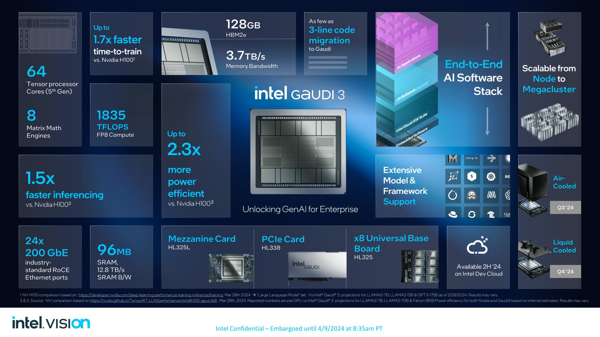
The latest iteration of Gaudi will be launching in the third quarter of 2024, and Intel is already shipping samples to customers now. The hardware itself is something of a mixed bag in some respects (more on that in a second), but with 1835 TFLOPS of FP8 compute throughput, Intel believes it’s going to be more than enough to carve off a piece of the expansive (and expensive) AI market for themselves. Based on their internal benchmarks, the company expects to be able beat NVIDIA’s flagship Hx00 Hopper architecture accelerators in at least some critical large language models, which will open the door to Intel grabbing a larger piece of the AI accelerator market at a critical time in the industry, and a moment when there simply isn’t enough NVIDIA hardware to go around.
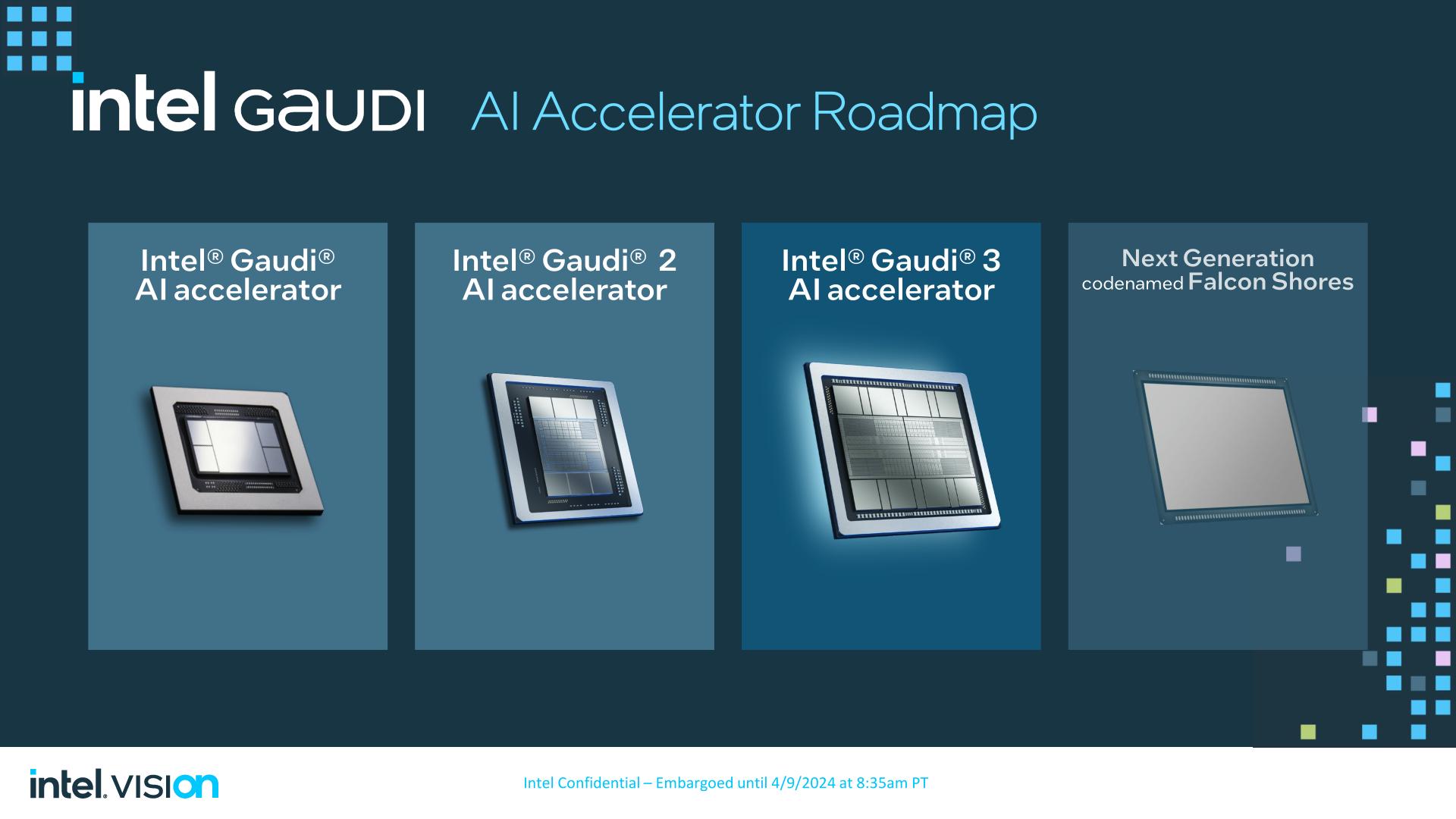
The upcoming launch of Gaudi 3 also comes amidst a change in how Intel is positioning its AI accelerator products – one that has seen the Gaudi lineup elevated to Intel’s flagship server accelerator. Traditionally downplayed in favor of Intel’s GPU Data Center Max products (Ponte Vecchio), Habana Labs and Gaudi have gained a new respect within Intel following the cancellation of Rialto Bridge in favor of the 2025 release of Falcon Shores. In short, Intel doesn’t have any other new AI accelerator silicon coming out besides Gaudi 3, so Intel is going to war with the chip that it has.
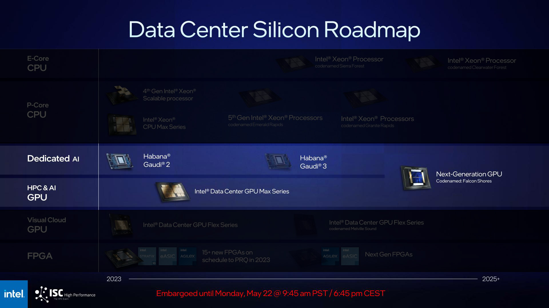
Above: Intel 2023 Data Center Silicon Roadmap, With GPUs
Which is not to knock Habana Labs or Gaudi 3 in advance. Intel thinks they can win here on performance; if they can, that’s a big deal. But this is a product that’s clearly been uplifted from a side-project under the Intel umbrella to a front-and-center processor. So the scope of Gaudi 3’s abilities, hardware, and what kind of markets Intel is chasing, is narrower than we’ve seen with some of their other flagship products.
| Gaudi Accelerator Specification Comparison | |||||
| Gaudi 3 | Gaudi 2 | Gaudi (1) | |||
| Matrix Math Engines | 8 | 2 | 1 | ||
| Tensor Cores | 64 | 24 | 8 | ||
| Clockspeed | ? | ? | ? | ||
| Memory Clock | 3.7Gbps HBM2e | 3.27Gbps HBM2e | 2Gbps HBM2 | ||
| Memory Bus Width | 2x 4096-bit | 6144-bit | 4096-bit | ||
| Memory Bandwidth | 3.7TB/sec | 2.45TB/sec | 1TB/sec | ||
| VRAM | 128GB (2x 64GB) |
96GB | 32GB | ||
| FP8 Matrix | 1835 TFLOPS | 865 TFLOPS | N/A | ||
| BF16 Matrix | 1835 TFLOPS | 432 TFLOPS | ? TFLOPS | ||
| Interconnect | 200Gb Ethernet 24 Links (600GB/sec) |
100Gb Ethernet 24 Links (300GB/sec) |
100Gb Ethernet 10 Links (120GB/sec) |
||
| Processor | Gaudi 3 | Gaudi 2 | Gaudi (1) | ||
| Transistor Count | 2x (A lot) | ? | ? | ||
| TDP | 900W | 600W | 350W | ||
| Manufacturing Process | TSMC 5nm | TSMC 7nm | TSMC 16nm | ||
| Interface | OAM 2.0 | OAM 1.1 | OAM | ||
Diving in to the hardware itself, let’s take a look at Gaudi 3.
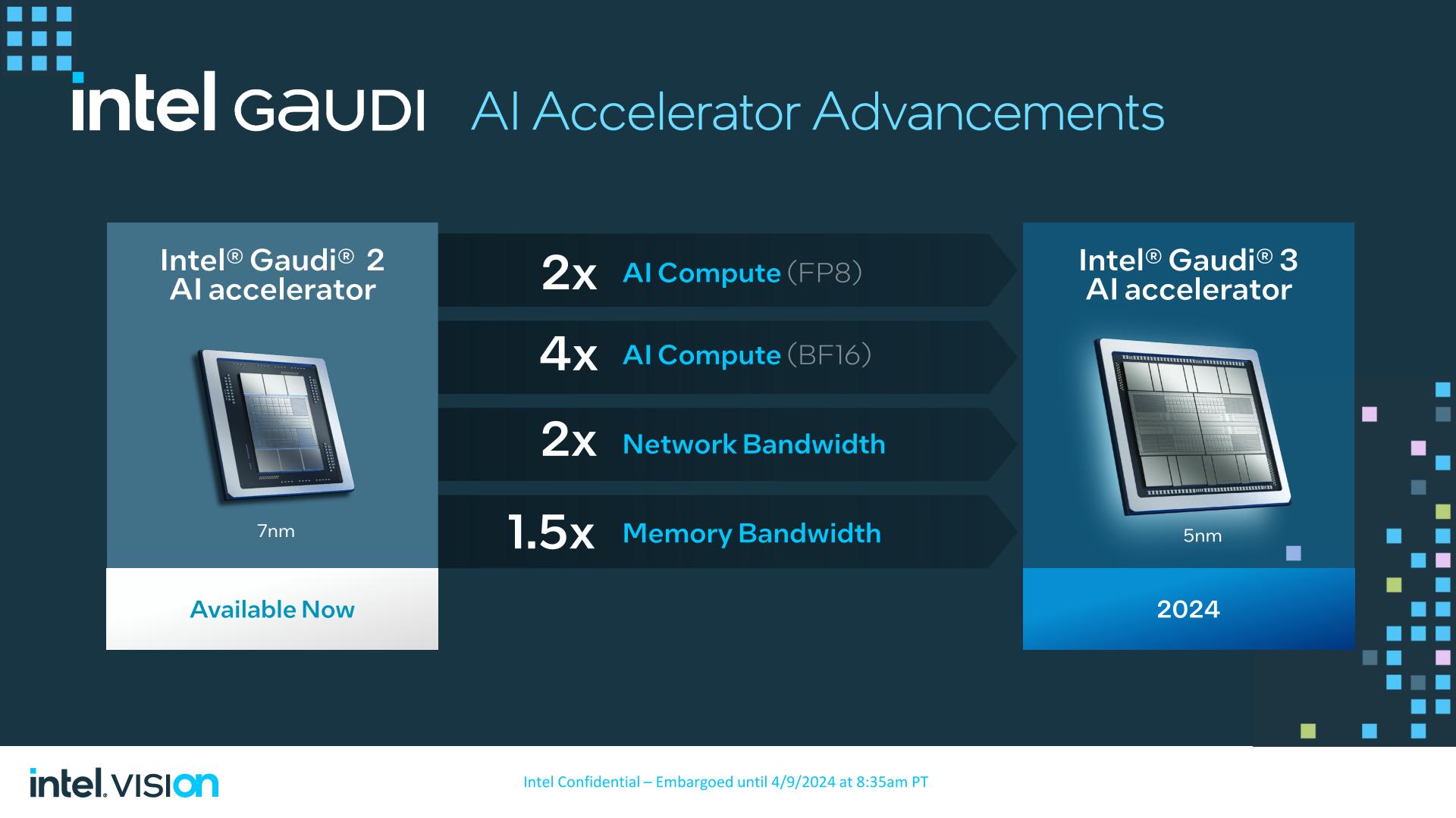
Gaudi 3 is a direct evolution of the Gaudi 2 hardware. Habana Labs has settled on an architecture they like and consider successful, so Gaudi 3 isn’t orchestrating a massive overhaul of their architecture (that will come with Falcon Shores). The flip side to that, however, is that there’s not a ton to talk about here in terms of new features – or features that Intel wants to disclose, at least – so at a high level, Gaudi 3 is more of a good thing.
With the previous-generation Gaudi 2 accelerator being built on TSMC’s 7nm process, Habana has brought Gaudi 3 to the newer 5nm process. The Gaudi 3 die, in turn, has added a modest amount of computational hardware, expanding from 2 Matrix Math Engines and 24 Tensor Cores to 4 Matrix Math Engines and 32 Tensor cores. Given the limited architecture changes with Gaudi 3, I’m presuming that these tensor cores are still 256 byte-wide VLIW SIMD units, as they were in Gaudi 2.
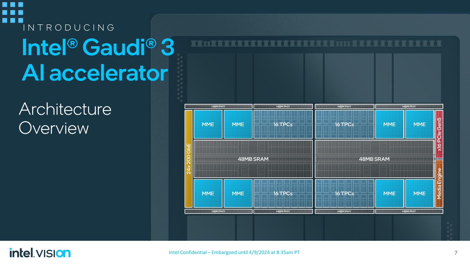
While Intel isn’t disclosing the total transistor count of the Gaudi 3 die, the limited addition of new hardware has made Gaudi 3 small enough that Intel has been able to pack two dies on to a single chip, making the full Gaudi 3 accelerator a dual-die setup. Similar to NVIDIA’s recently announced Blackwell accelerator, two identical dies are placed on a single package, and are connected via a high bandwidth link in order to give the chip a unified memory address space. According to Intel, the combined dies will behave as a single chip, though as the company isn’t disclosing any significant details on the die-to-die link connecting the chips, it remains unclear just how much bandwidth is actually available to cross the dies, and at what latency.
In a rarity for the Habana team, they have disclosed the total throughput of the chip for FP8 precision: 1835 TFLOPS, which is twice the FP8 performance of Gaudi 2. More interesting is that BF16 performance has apparently increased by 4x over Gaudi 2, however Intel hasn’t disclosed an official throughput number for that mode, or what architectural changes have led to that improvement. Either way, Intel needs to maximize the performance of Gaudi 3 if they’re going to carve off a piece of the AI market for themselves.
Update, 3pm: Habana has since published a whitepaper for Gaudi 3 this afternoon, which includes a few more details on the architecture and its performance. The chip's BF16 performance is now 1835 TFLOPS, putting it at parity with FP8 performance. This is somewhat surprising to see, since most architectures can execute FP8 at twice their FP16/BF16 rate. Either way, this puts Gaudi 3 in a better position than we first thought for higher precision BF16 training.
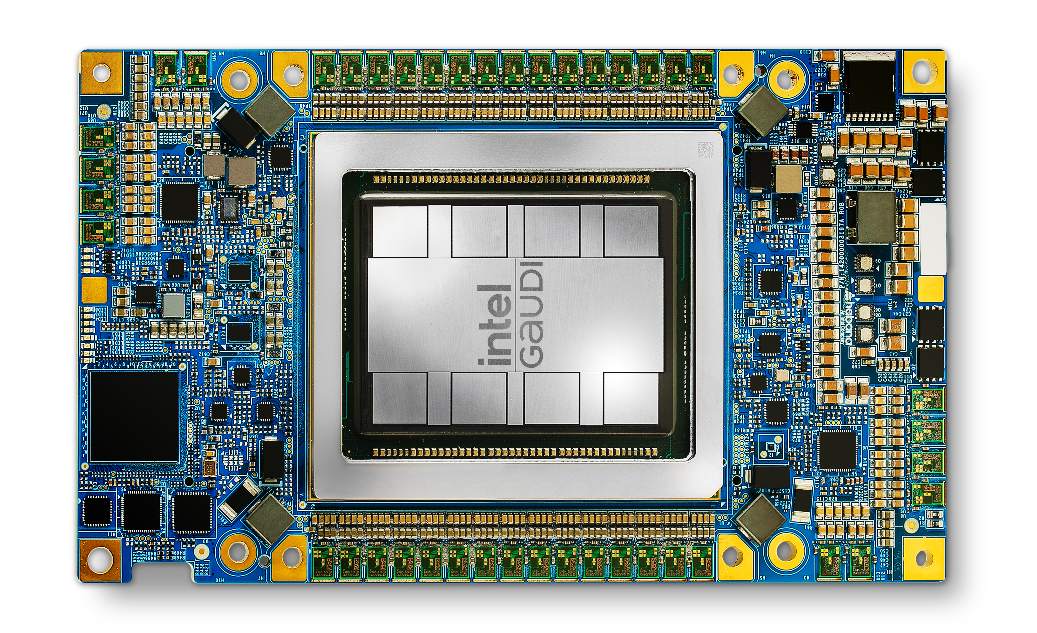
Feeding the beast is an oddly outdated HBM2e memory controller, the same memory type supported by Gaudi 2. While Intel is probably a smidge too early for HBM3E, I am very surprised not to see HBM3 supported, both for the greater memory bandwidth and greater memory capacity the HBM3 lineage affords. As a result of sticking with HBM2e, the highest capacity stacks available are 16GB, giving the accelerator a total of 128GB of memory. This is clocked at 3.7Gbps/pin, for a total memory bandwidth of 3.7TB/second. Each Gaudi 3 die offers 4 HBM2e PHYs, bringing the chip’s total to 8 stacks of memory.
Meanwhile, each Gaudi 3 die has 48MB of SRAM on-board, giving the complete chip 96MB of SRAM. According to Intel, the aggregate SRAM bandwidth is 12.8TB/second.
Intel is not disclosing the clockspeed of the Gaudi 3 accelerator (nor did they ever disclose Gaudi 2’s, for that matter). However given that Intel has more than doubled the hardware on-hand, we’re likely looking at lower clockspeeds overall. Even with the smaller 5nm die, two dies means a whole lot more transistors to feed, and not a ton of additional power to do it.
On that note, the TDP for the basic, air-cooled Gaudi 3 accelerator is 900 Watts, 50% higher than the 600W limit of its predecessor. Intel is making use of the OAM 2.0 form factor here, which affords a higher power limit than OAM 1.x (700W). However, Intel is also developing and qualifying liquid-cooled versions of Gaudi 3, which will offer higher performance in exchange for even higher TDPs. All forms of Gaudi 3 will use PCIe backhaul to connect to their host CPU, with Gaudi 3 sporting a PCIe Gen 5 x16 link.
Broadly speaking, the limited details on the Gaudi architecture remind me a great deal of AMD’s Instinct MI250X accelerator. That CDNA 2 part was in many ways a pair of die-shrunk MI100s placed together on a single chip, bringing few new architectural features, but a whole lot more silicon to do the heavy lifting. Critically, however, MI250X presented itself as two accelerators (despite the Infinity Fabric links between the dies), whereas Gaudi 3 is supposed to behave as a single unified accelerator.
Networking: Ethernet Taken To The Extreme
Outside of the core architecture of the Gaudi 3, Habana’s other big technological upgrade with Gaudi 3 has been on the I/O side of matters. Going back to the earliest days of Gaudi, Habana has relied on an all-Ethernet architecture for their chips, using Ethernet for both on-node chip-to-chip connectivity, and scale-out node-to-node connectivity. It is essentially the inverse of what NVIDIA has done, scaling Ethernet down to the chip level, rather than scaling NVLink up to the rack level.
Gaudi 2 offered 24 100Gb Ethernet links per chip; Gaudi 3 doubles the bandwidth of those links to 200Gb/second, giving the chip a total external Ethernet I/O bandwidth of 8.4TB/second cumulative up/down.
The recommended topology for Gaudi 3 – and what Intel will be employing in their own baseboards – is a 21/3 split. 21 links will be used for on-node, chip-to-chip connectivity, with 3 links going to each of the other 7 Gaudi 3 accelerators on a fully populated 8-way node.
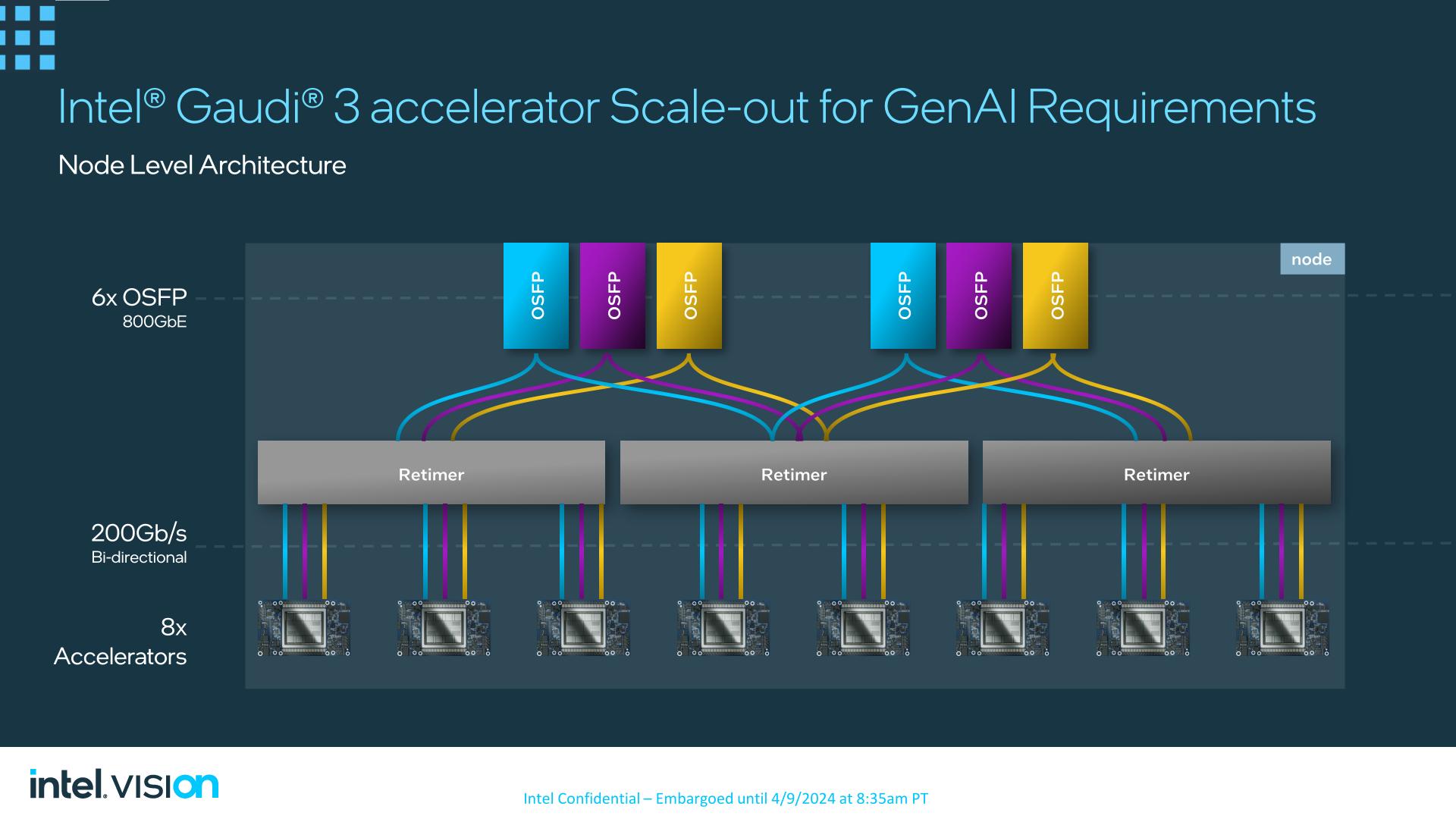
The remaining 3 links from each chip, meanwhile, will be used to feed a sextet of 800Gb Octal Small Form Factor Pluggable (OSFP) Ethernet links. Via the use of retimers, the ports will be split up in blocks of two, and then balanced over 5 accelerators.
Ultimately, Intel is looking to push the scalability of Gaudi 3 here, both in terms of performance and marketability. With the largest of LLMs requiring many nodes to be linked together to form a single cluster to provide the necessary memory and compute performance for training, the biggest customers that Intel is chasing with Gaudi 3 will need an AI accelerator that can scale out to these large sizes – and thus giving Intel plenty of opportunity to sell an equally large number of accelerators. All the while, by embracing a pure Ethernet setup, Intel is banking on winning over customers who don’t want to invest in proprietary/alternative interconnects such as InfiniBand.
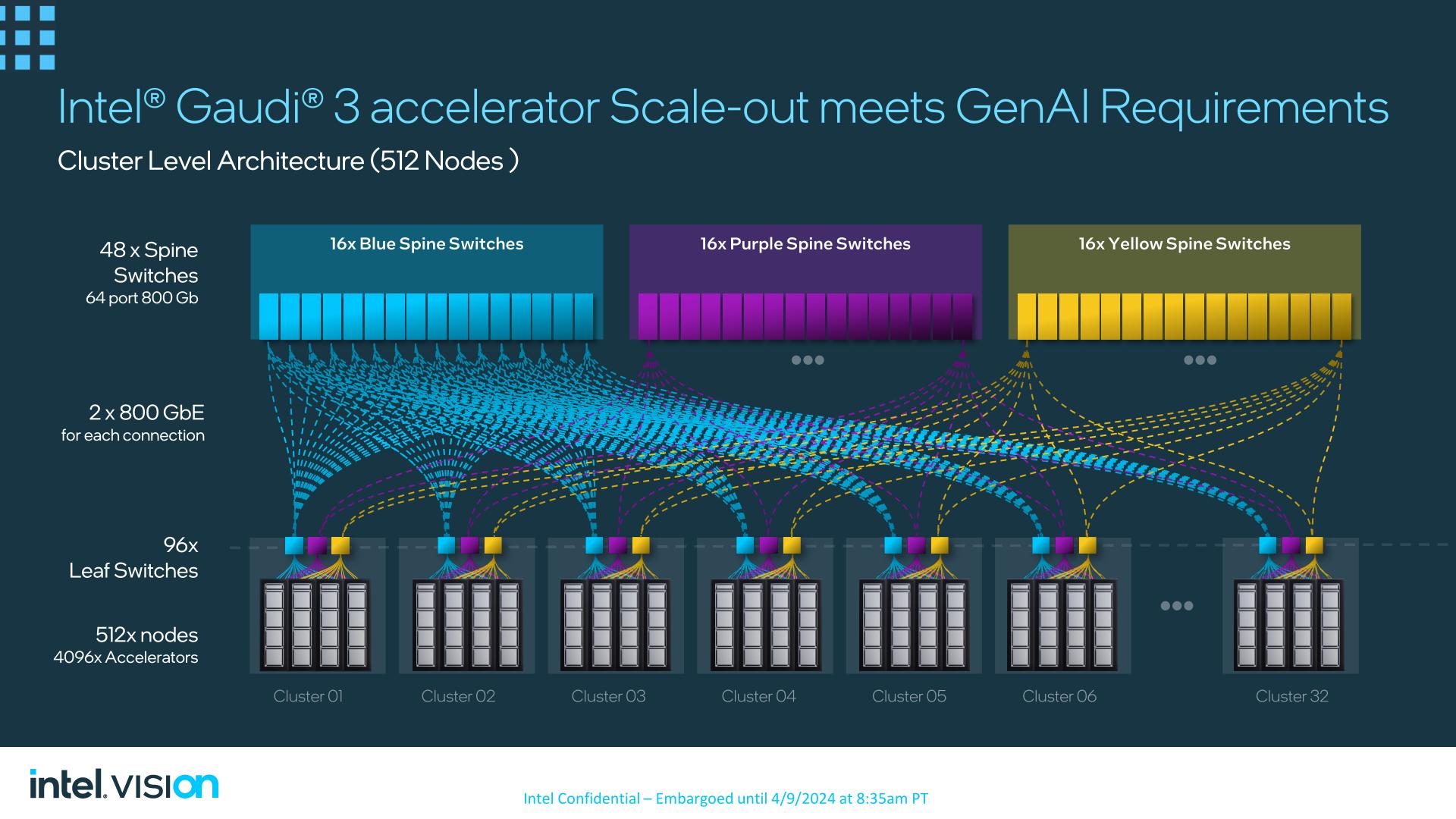
Ultimately, Intel has networking topologies for as many as 512 nodes already developed, using 48 spine switches to connect up to 32 clusters – each of which houses 16 nodes. And according to Intel, Gaudi 3 can still scale further than that, out to thousands of nodes.
Performance: Beating H100 At Llamas and Falcons
Throughout the lifetime of the Gaudi accelerators, Intel and Habana have preferred to focus on talking about the performance of the chips instead of just the specifications, and for Gaudi 3 that is not changing. With the bulk of Vision’s attendees being business clientele, Intel is looking to make a splash with benchmark-based performance figures that demonstrate what Gaudi 3 can actually do.
I’m not going to spend too much time going over these since they’re primarily competitive performance claims that we can’t validate. But it’s noteworthy here that the Gaudi team opted to go straight at NVIDIA here by using their own benchmarks and result sets. In other words, the Gaudi performance figures provided by Intel are plotted against NVIDIA’s own self-reported figures, rather than Intel cooking up scenarios to disadvantage NVIDIA. That said, it must also be noted that these are performance projections, and not measured performance of assembled systems (and I doubt Intel has 8192 Gaudi 3s sitting around for this).
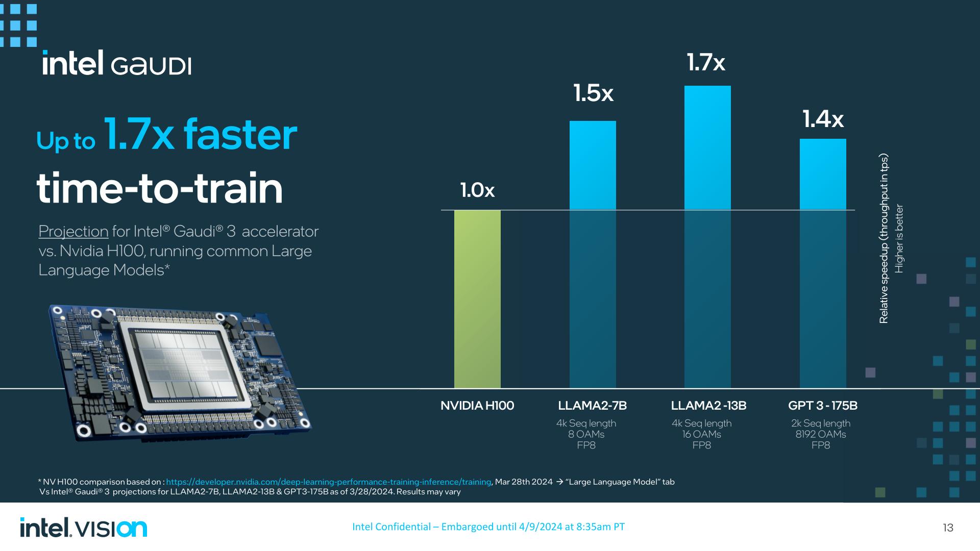
Compared to H100, Intel is claiming that Gaudi 3 should beat H100 by up to 1.7x in training Llama2-13B in a 16 accelerator cluster at FP8 precision. Even though H100 is coming up on 2 years old, beating H100 at training anything by a significant degree would be a big win for Intel if it pans out.
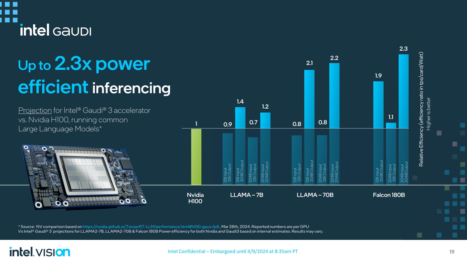
Meanwhile, Intel is projecting 1.3x to 1.5x the inferencing performance of H200/H100 with Gaudi 3, and perhaps most notably, at up to 2.3x the power efficiency.
As always, however, the devil is in the details. Intel still loses to the H100 at times in these inference workloads – particularly those without 2K outputs – so the Gaudi 3 is far from a clean sweep. And, of course, there are all of the benchmark results that Intel isn’t promoting.
To Intel’s credit, however, they are the only other major hardware manufacturer who has been providing MLPerf results as of late. So however Gaudi 3 will perform (and how Gaudi 2 currently performs), they have been far more above-board than most in publishing results for industry-standard tests.
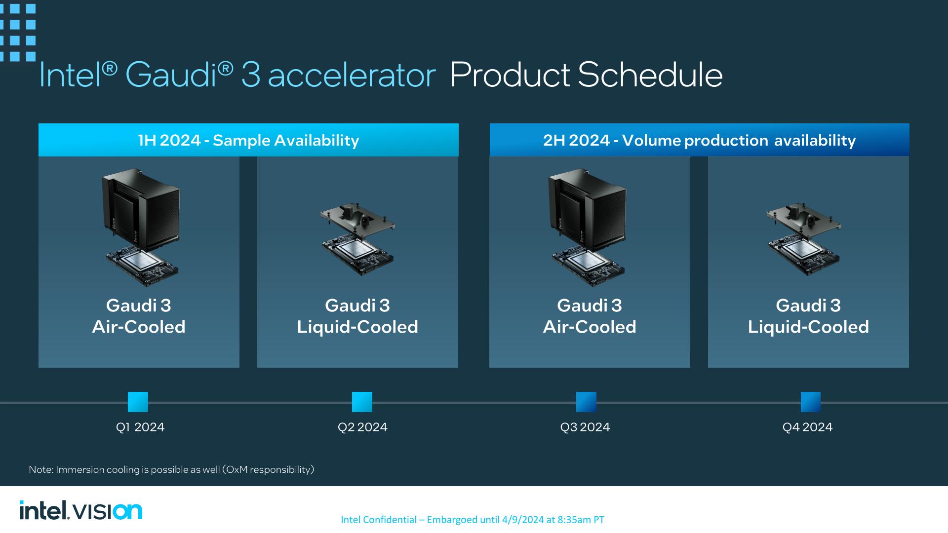
OAM and PCIe Cards Launching In Second-Half of 2024
Wrapping things up, Intel will be releasing their first Gaudi 3 products in the next quarter. The company already has air-cooled versions of the OEAM accelerator in their labs for qualification and out to customers for sampling, meanwhile the liquid-cooled versions will be sampling this quarter.
Finally, in a first time for the Gaudi team, Intel will be offering a version of Gaudi 3 in a more traditional PCIe form factor as well. The HL-338 card is a 10.5-inch full height dual-slot PCIe card. It offers all of the same hardware as the OAM Gaudi 3, right on down to the peak performance of 1835 TFLOPS FP8. However it will ship with a far more PCIe-slot friendly TDP of 600 Watts – 300 Watts less than the OAM card – so sustained performance should be notably lower.
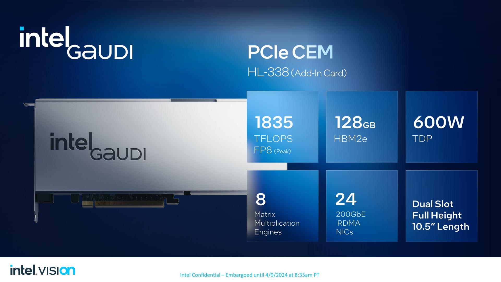
Though not pictured in Intel’s slide, the PCIe cards offer two 400Gb Ethernet ports for scale-out configurations. Meanwhile Intel will be offering a “top board” for the PCIe cards that, similar to NVIDIA’s NVLink bridges, can link up to 4 of them for inter-card communication. The OAM form factor will remain the way to go for both highest performance on a per-accelerator basis and to maximize scale-out potential, but for customers who need something to plug and go in traditional PCIe slots, there is finally an option for that for a Gaudi accelerator.
The PCIe version of the Gaudi 3 is set to launch in the 4th quarter of this year, alongside the liquid cooled version of the OAM module.


21 Comments
View All Comments
trivik12 - Tuesday, April 9, 2024 - link
This is not firing on all cylinders. Should have used HBM3 and TSMC N3B or Intel 3. This is the most important product in today's times and Intel is being too conservative with their choices. Its not going to make much of a splash in the market. Hopefully Falcon Shores goes all in with Intel 18A, HBM 3E and everything else.elmagio - Tuesday, April 9, 2024 - link
A chip that size on a 3nm node would cost so much and have yields so catastrophic they'd probably lose money even at the insane pricing of AI chips.Regardless, it's most likely a foolish endeavor to bet everything on producing the *best* AI chip at any cost today considering Nvidia's headstart. It's a much smarter play to aim for somewhere between a H100 and H200 at acceptable costs because that's actually a realistic goal.
Threska - Tuesday, April 9, 2024 - link
AI in a lot of IoT.Silma - Wednesday, April 10, 2024 - link
Even NVIDIA is going for TSMC's 4nm, not the 3nm.There must be a reason. Either low yield or cost or Apple's exclusivity.
Regarding memory, it's strange. I wonder if Intel's decision is based on not wanting to spend money, or if there aren't enough HBM3/E available on the market. After all, NVIDIA surely did secure enough memory chips for its accelerators.
Bruzzone - Friday, April 19, 2024 - link
Depreciated process cost TSMC 4__. mbKevin G - Tuesday, April 9, 2024 - link
While a step up from Gaudi 2, this seems too little too late given that nVidia's Blackwell was announced beforehand. Granted neither of these are shipping with the common comparison point being Hopper. While faster than that comparison point via Intel's chosen benchmarks, it really has to do better than Blackwell which doesn't seem likely given what nVidia has said about its own generational improvements.The other huge factor here is interconnects to scale up. Ethernet is a more commodity choice but does permit scaling upward to huge numbers and has benefits of being able to interop with other systems/accelerators. It would have been nice if Intel hadn't sold off their Ethernet switch division 15 months ago as there is a good pairing of technologies here. Essentially throw a newer Barefoot switch ASIC on the base board and leverage a 100GbaseKX style spec to link everything together on the board with massive uplink bandwidth to go outside of the node.
Scaling counts upward is supposed to be Gaudi 3's specialty and Intel should power and price these to enable this and permit clusters outperform those form their competitors. If you can't win on a 1:1 battle, make it a 2:1 battle where you can win. At 900W per board, there are costs and cooling complexities there if Intel is driving the design hard. Lowering clocks and voltages maybe warranted if operating at 600W can do 85% of the performance at 900W. It'd make things cheaper to cool and maintain. There is a niche opportunity win to be able to replace existing clusters without needing to go to liquid cooling which given Intel's position should press hard. Similarly Intlel should be undercutting its competitors in price in an effort to gain market share here while emphasizing performance per dollar (which includes the power side of things). I don't see Intel going in this direction for various reasons and they'll wind up with another 'success' like Ponte Vecchio on their hands.
Blastdoor - Tuesday, April 9, 2024 - link
Kind of a bummer that Intel isn’t manufacturing this themselves, but rather relying on TSMC.ballsystemlord - Tuesday, April 9, 2024 - link
Why sell off their fabs when they can outsource both their production capabilities and needs? (sarcasm).name99 - Saturday, April 20, 2024 - link
I think the word you mean is “red flag”, not “bummer”…soaringrocks - Sunday, April 21, 2024 - link
I'm guessing that with all those Ethernet lanes this chip will not be from an Intel Fab. Intel Fabs are great, but Mixed Signal IP required for Ethernet was never a strong point for them. It's expensive to develop and they don't make enough designs to amortize the high cost of developing the IP.