Intel Goes Full XPU: Falcon Shores to Combine x86 and Xe For Supercomputers
by Ryan Smith on February 17, 2022 2:30 PM EST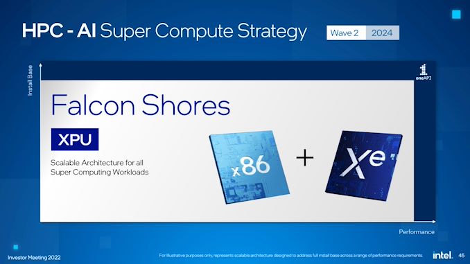
One of Intel’s more interesting initiatives over the past few years has been XPU – the idea of using a variety of compute architectures in order to best meet the execution needs of a single workload. In practice, this has led to Intel developing everything from CPUs and GPUs to more specialty hardware like FPGAs and VPUs. All of this hardware, in turn, is overseen at the software level by Intel’s oneAPI software stack, which is designed to abstract away many of the hardware differences to allow easier multi-architecture development.
Intel has always indicated that their XPU initiative was just a beginning, and as part of today’s annual investor meeting, Intel is finally disclosing the next step in the evolution of the XPU concept with a new project codenamed Falcon Shores. Aimed at the supercomputing/HPC market, Falcon Shores is a new processor architecture that will combine x86 CPU and Xe GPU hardware into a single Xeon socket chip. And when it is released in 2024, Intel is expecting it to offer better than 5x the performance-per-watt and 5x the memory capacity of their current platforms.
At a very high level, Falcon Shores appears to be an HPC-grade APU/SoC/XPU for servers. While Intel is offering only the barest of details at this time, the company is being upfront in that they are combining x86 CPU and Xe GPU hardware into a single chip, with an eye on leveraging the synergy between the two. And, given the mention of advanced packaging technologies, it’s a safe bet that Intel has something more complex than a monolithic die planned, be it separate CPU/GPU tiles, HBM memory (e.g. Sapphire Rapids), or something else entirely.
Diving a bit deeper, while integrating discrete components often pays benefits over the long run, the nature of the announcement strongly indicates that there’s more to Intel’s plan here than just integrating a CPU and GPU into a single chip (something they already do today in consumer parts). Rather, the presentation from Raja Koduri, Intel’s SVP and GM of the Accelerated Computing Systems and Graphics (AXG) Group, makes it clear that Intel is looking to go after the market for HPC users with absolutely massive datasets – the kind that can’t easily fit into the relatively limited memory capacity of a discrete GPU.
A singular chip, in comparison, would be much better prepared to work from large pools of DDR memory without having to (relatively) slowly shuffle data in and out of VRAM, which remains a drawback of discrete GPUs today. In those cases, even with high speed interfaces like NVLink and AMD’s Infinity Fabric, the latency and bandwidth penalties of going between the CPU and GPU remain quite high compared to the speed at which HPC-class processors can actually manipulate data, so making that link as short as physically possible can potentially offer performance and energy savings.

Meanwhile, Intel is also touting Falcon Shores as offering a flexible ratio between x86 and Xe cores. The devil is in the details here, but at a high level it sounds like the company is looking at offering multiple SKUs with different numbers of cores – likely enabled by varying the number of x86 and Xe titles.
From a hardware perspective then, Intel seems to be planning to throw most of their next-generation technologies at Falcon Shores, which is fitting for its supercomputing target market. The chip is slated to be built on an “angstrom era process”, which given the 2024 date is likely Intel’s 20A process. And along with future x86/Xe cores, will also incorporate what Intel is calling “extreme bandwidth shared memory”.
With all of that tech underpinning Falcon Shores, Intel is currently projecting a 5x increase over their current-generation products in several metrics. This includes a 5x increase in performance-per-watt, a 5x increase in compute density for a single (Xeon) socket, a 5x increase in memory capacity, and a 5x increase in memory bandwidth. In short, the company has high expectations for the performance of Falcon Shores, which is fitting given the highly competitive HPC market it’s slated for.
And perhaps most interestingly of all, to get that performance Intel isn’t just tackling things from the raw hardware throughput side of matters. The Falcon Shores announcement also mentions that developers will have access to a "vastly simplified GPU programming model" for the chip, indicating that Intel isn’t just slapping some Xe cores into the chip and calling it a day. Just what this entails remains to be seen, but simplifying GPU programming remains a major goal in the GPU computing industry, especially for heterogeneous processors that combine CPU and GPU processing. Making it easier to program these high throughput chips not only makes them more accessible to developers, but reducing/eliminating synchronization and data preparation requirements can also go a long way towards improving performance.
Like everything else being announced as part of today’s investor meeting, this announcement is more of a teaser for Intel. So expect to hear a lot more about Falcon Shores over the next couple of years as Intel continues their work to bringing it to market.
Source: Intel


28 Comments
View All Comments
name99 - Thursday, February 17, 2022 - link
"All of this hardware, in turn, is overseen at the software level by Intel’s oneAPI software stack, which is designed to abstract away many of the hardware differences to allow easier multi-architecture development."Except that, apparently, it doesn't.
I was recently part of a Twitter thread complaining that the primary reason Gaudi (and earlier Nervana) were gaining little traction was the absence of decent SW. I raised oneAPI and was told that it did nothing that was actually of interest to the serious large-scale NNU teams.
I know very little about oneAPI or NNU hardware, so I have no comment. But it does feel like oneAPI (like so much from Intel these days) exists a lot more on marketing slides and a lot less in actual customers hands.
edzieba - Monday, February 21, 2022 - link
A twitter complaints thread is probably not the best source for API adoption information.mode_13h - Sunday, February 27, 2022 - link
> it does feel like oneAPI (like so much from Intel these days) exists a lot more> on marketing slides and a lot less in actual customers hands.
Not exactly. At some level, it's a CPU/GPU API, being built upon SYCL and Data-Parallel C++. Their OpenVINO framework has a backend for it that supports their GPUs, which I know because we're using it.
Surprisingly, it seems OpenVINO still lacks backends for any Nervana or Habana ASIC, but they do have some level of support for Movidius and their GNA.
https://docs.openvino.ai/latest/openvino_docs_IE_D...
ballsystemlord - Thursday, February 17, 2022 - link
Sort of like Intel will be on 10nm within the next year? ;)michael2k - Friday, February 18, 2022 - link
What do you mean? They’ve been on 10nm forever and just renamed their latest 10nm node I7ballsystemlord - Sunday, March 6, 2022 - link
I was poking fun at Intel's recent slip with respect to the launch of their 10nm node. I was contrasting their lack of staying on schedule there with their current plans being likely to slip.JayNor - Thursday, February 17, 2022 - link
The servethehome article, "Intel AXG on Falcon Shores Arctic Sound-M and Future Products at Investor Meeting 2022", mentioned that in a prior interview Raja made a note "LightBender", in reference to Falcon Shores' leading IO ... his interpretation that this meant Silicon Photonics.I believe late 2024 to 2025 does match up with an in-package photonics roadmap Intel's Blum has presented.
Kevin G - Friday, February 18, 2022 - link
Silicon photonics is one of those aces Intel has had up their sleeves for awhile. Thus far they've only been leveraging that to produce some optical transceivers for Cisco.Intel has been buying up networking companies with an eye of using their own advanced manufacturing and packaging to move those acquisitions forward. Intel's tile strategy will pay off here as the switch IO can be built using their silicon photonics as a discrete tile while the switch ASIC portion will be their own die. Then put in a few x86 dies for management and some memory controller dies to round out the product for the networking segment.
For the HPC side of things, those same tile used in the networking segment can be fully integrated as well for more internode bandwidth and lower latency. The switch ASIC portion wouldn't necessarily have to be Ethernet based as it could be something unique like PCIe over optics that leverages CXL to build a flat memory space and handle coherency.
name99 - Friday, February 18, 2022 - link
Or Silicon Photonics is the next Optane, a theoretically promising technology that Intel will fsck up through a combination of management incompetence, attempted market segmentation, tying it to intel products rather than allowing it to become generic technology, and so on...emvonline - Saturday, February 19, 2022 - link
I think the optane analogy is that Optane works, but few people want it and are willing to pay for it. So it doesnt matter and no one cares. Many people have Si photonics technology. Do people want it and are they willing to pay for it. Was Optane mentioned at the investor meeting? I didnt hear it