Insights into DDR5 Sub-timings and Latencies
by Dr. Ian Cutress on October 6, 2020 11:00 AM EST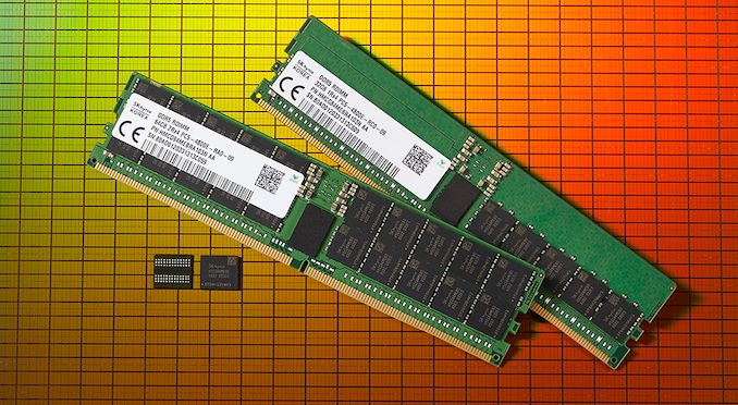
Today we posted a news article about SK hynix’s new DDR5 memory modules for customers – 64 GB registered modules running at DDR5-4800, aimed at the preview systems that the big hyperscalers start playing with 12-18 months before anyone else gets access to them. It is interesting to note that SK Hynix did not publish any sub-timing information about these modules, and as we look through the announcements made by the major memory manufacturers, one common theme has been a lack of detail about sub-timings. Today can present information across the full range of DDR5 specifications.
When discussing memory, there are a few metrics to consider:
- Type, e.g. DDR4, DDR5
- Capacity
- Power consumption / voltage
- Bandwidth
- Latency
- Price
- Persistence
When building a platform, a number of these factors all come into play – a system that implements oil and gas simulations might require terabytes of memory, regardless of power, of for smaller installations price might be the major concern. For specialist applications, persistent memory might be a focus, or a combination of bandwidth/latency will be key to driving performance.
In order for all these companies that build memory and systems to work together, a set of standards are developed by a consortium of all interested parties – this is called JEDEC. JEDEC creates the standards to ensure support for all compliant systems.
Users who are familiar with JEDEC specifications will note that consumer grade memory is often specified faster than what JEDEC lists – this is a feature in which processors that can support faster memory, when paired with memory qualified to be faster than JEDEC, can be paired together. This is why we see memory kits all the way up to DDR4-5000 in the market today that only work with a few select systems.
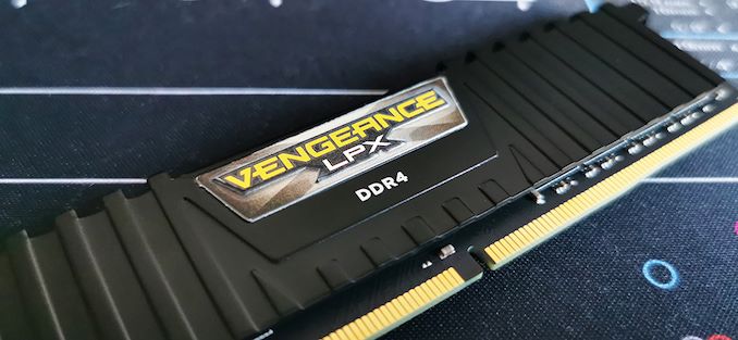
Read AnandTech’s Corsair DDR4-5000 Vengeance LPX Review
Super-Binned, Super Exclusive
For DDR4, JEDEC supports standards ranging from DDR4-1600 up to DDR4-3200. From the data rate, a peak transfer rate can be calculated (12.8 GB/s per channel for DDR4-1600, 25.6 GB/s per channel for DDR4-3200), however the latency requires additional information. The typical sub-timings offered with memory are:
- CAS: Column Address Strobe: the time between sending a column address and the response
- tRCD: Row to Column Delay: clock cycles to load a column when new row is opened
- tRP: Row Precharge Time: clock cycles to load data when wrong row is open
- tRAS: Row Active Time: minimum time between row active and precharge
These are typically reported as CAS-tRCD-tRP with tRAS sometimes added on. This means that in JEDEC’s DDR4 specification, the base DDR4-3200 metric allows for a 24-24-24 set of sub-timings. For latency calculations, we need both the data rate (3200 MT/s) and the CAS (24 clocks) to calculate the CAS in terms of nanoseconds, the real world latency (in this case, 15 nanoseconds).
The combination of data rate and CAS Latency has been used to compare single access latency numbers for memory over the years. Moving from the early iterations of DRAM, both data access rates and single access latencies have improved. However recently, due to physical limitations, while data rate has been increasing, access latency has been roughly consistent.
| Memory and Bandwidth, up to DDR4 | |||||
| AnandTech | Data Rate MT/s |
Bandwidth GB/s |
CAS (clk) |
Latency (ns) |
|
| SDR | |||||
| SDR | 100 | 100 | 0.80 | 3 | 24.00 |
| 133 | 133 | 1.07 | 3 | 22.50 | |
| DDR | |||||
| DDR | 200 | 200 | 1.60 | 2 | 20.00 |
| 333 | 333 | 2.67 | 2.5 | 15.00 | |
| 400 | 400 | 3.20 | 3 | 15.00 | |
| DDR 2 | |||||
| DDR2 | 400 | 400 | 3.20 | 5 | 25.00 |
| 667 | 667 | 5.33 | 5 | 15.00 | |
| 800 | 800 | 6.40 | 6 | 15.00 | |
| DDR 3 | |||||
| DDR3 | 800 | 800 | 6.40 | 6 | 15.00 |
| 1066 | 1066 | 8.53 | 8 | 15.00 | |
| 1333 | 1333 | 10.67 | 9 | 13.50 | |
| 1600 | 1600 | 12.80 | 11 | 13.75 | |
| 1866 | 1866 | 14.93 | 13 | 13.93 | |
| 2133 | 2133 | 17.07 | 14 | 13.13 | |
| DDR 4 | |||||
| DDR4 | 1600 | 1600 | 12.80 | 11 | 13.75 |
| 1866 | 1866 | 14.93 | 13 | 13.92 | |
| 2133 | 2133 | 17.07 | 15 | 14.06 | |
| 2400 | 2400 | 19.20 | 17 | 14.17 | |
| 2666 | 2666 | 21.33 | 19 | 14.25 | |
| 2933 | 2933 | 23.46 | 21 | 14.32 | |
| 3200 | 3200 | 25.20 | 22 | 13.75 | |
| *Not all of these are JEDEC Standards | |||||
Pivoting to DDR5, JEDEC has enabled standards ranging from DDR5-3200 to DDR5-6400. It also has placeholders up to DDR5-8000, however the specifics of those standards are still a work in progress. At the end of DDR3, and through DDR4, JEDEC introduced additional sub-timing specifications for each data rate - for each of the data rates, JEDEC has specified an ‘A’ fast standard, a ‘B’ common standard, and a ‘C’ looser standard – technically the looser standard is more applicable to higher capacity modules. It means that each data rate can cast a wide range of performance based on the quality of the silicon used.
Starting with the lowest data rate, the DDR5-3200A standard supports 22-22-22 sub-timings. At a theoretical peak of 25.6 GB/s bandwidth per channel, this equates to a single access latency of 13.75 nanoseconds.
If we look at SK Hynix’s announcement of DDR5-4800, this could be DDR5-4800B which supports 40-40-40 sub-timings, for a theoretical peak bandwidth of 38.4 GB/s per channel and a single access latency of 16.67 nanoseconds.
Here is the full list, from DDR5-3200 to DDR5-6400, including some of the extra standards not yet finalized.
| DDR5 JEDEC Specifications | |||||||
| AnandTech | Data Rate MT/s |
CL* |
Peak BW GB/s |
Latency (ns) |
|||
| DDR5-3200 | A | 3200 | 22 | 22 | 22 | 25.60 | 13.75 |
| B | 26 | 26 | 26 | 16.25 | |||
| C | 28 | 28 | 28 | 17.50 | |||
| DDR5-3600 | A | 3600 | 26 | 26 | 26 | 28.80 | 14.44 |
| B | 30 | 30 | 30 | 16.67 | |||
| C | 32 | 32 | 32 | 17.78 | |||
| DDR5-4000 | A | 4000 | 28 | 28 | 28 | 32.00 | 14.00 |
| B | 32 | 32 | 32 | 16.00 | |||
| C | 36 | 36 | 36 | 18.00 | |||
| DDR5-4400 | A | 4400 | 32 | 32 | 32 | 35.20 | 14.55 |
| B | 36 | 36 | 36 | 16.36 | |||
| C | 40 | 40 | 40 | 18.18 | |||
| DDR5-4800 | A | 4800 | 34 | 34 | 34 | 38.40 | 14.17 |
| B | 40 | 40 | 40 | 16.67 | |||
| C | 42 | 42 | 42 | 17.50 | |||
| DDR5-5200 | A | 5200 | 38 | 38 | 38 | 41.60 | 14.62 |
| B | 42 | 42 | 42 | 16.15 | |||
| C | 46 | 46 | 46 | 17.69 | |||
| DDR5-5600 | A | 5600 | 40 | 40 | 40 | 44.80 | 14.29 |
| B | 46 | 46 | 46 | 16.43 | |||
| C | 50 | 50 | 50 | 17.86 | |||
| DDR5-6000 | A | 6000 | 42 | 42 | 42 | 48.00 | 14.00 |
| B | 50 | 50 | 50 | 16.67 | |||
| C | 54 | 54 | 54 | 18.00 | |||
| DDR5-6400 | A | 6400 | 46 | 46 | 46 | 51.20 | 14.38 |
| B | 52 | 52 | 52 | 16.25 | |||
| C | 56 | 56 | 56 | 17.50 | |||
| Future Bins | |||||||
| DDR5-6800 | 6800 | 54.40 | |||||
| DDR5-7200 | 7200 | 57.60 | |||||
| DDR5-7600 | 7600 | 60.80 | |||||
| DDR5-8000 | 8000 | 64.00 | |||||
| DDR5-8400 | 8400 | 67.20 | |||||
You may remember our report in May 2018, where Cadence and Micron showed off some DDR5-4400 memory in a test platform. We were able to determine from the photographs provided that this system was running at a CAS Latency of 42 clocks. Since then, the JEDEC standard has come down in that speed bracket to support 32-40 clocks, indicating the evolution of the platform.
The table above is a bit cumbersome, so here's the same table showing only the 'A' fastest specifications for each data rate. This likely applies for any installation of the equivalent of 1 module per channel.
| JEDEC DDR5-A Specifications | |||||||
| AnandTech | Data Rate MT/s |
CL |
Peak BW GB/s |
Latency (ns) |
|||
| DDR5-3200 | A | 3200 | 22 | 22 | 22 | 25.60 | 13.75 |
| DDR5-3600 | A | 3600 | 26 | 26 | 26 | 28.80 | 14.44 |
| DDR5-4000 | A | 4000 | 28 | 28 | 28 | 32.00 | 14.00 |
| DDR5-4400 | A | 4400 | 32 | 32 | 32 | 35.20 | 14.55 |
| DDR5-4800 | A | 4800 | 34 | 34 | 34 | 38.40 | 14.17 |
| DDR5-5200 | A | 5200 | 38 | 38 | 38 | 41.60 | 14.62 |
| DDR5-5600 | A | 5600 | 40 | 40 | 40 | 44.80 | 14.29 |
| DDR5-6000 | A | 6000 | 42 | 42 | 42 | 48.00 | 14.00 |
| DDR5-6400 | A | 6400 | 46 | 46 | 46 | 51.20 | 14.38 |
In terms of single access latency, we are ultimately not going to be any faster than we were by the end of the DDR3 era. DDR3-1866 at CL13 was already at 13.93 nanoseconds. This means that despite the increasing CAS latency values in clocks (going to CL46 at DDR5-6400), the actual single access latency is still roughly the same in real world time units.
It is interesting to note that the DDR5 specification has provision in the hardware registers for CAS Latencies from CL22 up to CL66. This might be interpolated to mean that even with a sufficiently binned DDR5 memory module, or with overclocking, CL22 might be the lowest possible for the hardware. We know that DDR5 now moves the voltage regulation for the memory onto the module, so that will be an additional area for memory manufacturers to differentiate themselves, especially when targeting the enthusiast market.
For users looking for an insight into how DRAM actually works, then I would like to direct you to our 2010 article entitled 'Everything You Always Wanted To Know About Memory (But Were Afraid To Ask)'. It's a great technical article that I still refer back to, and I still scratch my head over!
Source: JEDEC DDR5 Specification
Related Reading
- DDR5 Memory Specification Released: Setting the Stage for DDR5-6400 And Beyond
- SK Hynix: We're Planning for DDR5-8400 at 1.1 Volts
- Cadence DDR5 Update: Launching at 4800 MT/s, Over 12 DDR5 SoCs in Development
- Samsung to Produce DDR5 in 2021 (with EUV)
- Here's Some DDR5-4800: Hands-On First Look at Next Gen DRAM
- CES 2020: Micron Begins to Sample DDR5 RDIMMs with Server Partners
- SK Hynix Details DDR5-6400
- Keysight Reveals DDR5 Testing & Validation System
- SK Hynix Develops First 16 Gb DDR5-5200 Memory Chip, Demos DDR5 RDIMM
- Cadence & Micron DDR5 Update: 16 Gb Chips on Track for 2019
- Cadence and Micron Demo DDR5-4400 IMC and Memory, Due in 2019


87 Comments
View All Comments
AMDSuperFan - Tuesday, October 6, 2020 - link
Because of the modulation of an AMD chip using multi-chip module design, I would expect DDR-5 to be up to 10 x faster than DDR-4 on an AMD chip. The multi-chip modules should be able to consume much more bandwidth while at the same time using a new memory controller to really spruce things up. I once used 386 class of computer. Upgrading to the 486 class was very good and a big part was because of the new memory. Also, won't these new DDR-5 modules be up to double memory per chip? Could we not see 128GB memory chips in DDR-5?Ian Cutress - Tuesday, October 6, 2020 - link
10x faster? huh?On capacity, we've addressed that a few times, most recently in the post earlier today that's in the link in the first sentence of this post: https://www.anandtech.com/show/16142/ddr5-is-comin...
SarahKerrigan - Tuesday, October 6, 2020 - link
This is the same guy that has been posting over and over again on Intel laptop chips insisting that they're slower than Big Navi. He's an obvious troll.drexnx - Tuesday, October 6, 2020 - link
obvious troll or actually insane? at this point to me it's not clear.the sheer gibberish they post really can't be neatly defined as either...
Showtime - Tuesday, October 6, 2020 - link
He needs to be banned. This isn't AYMD on reddit. Bad enough with all the misinformation I read every else.Hifihedgehog - Tuesday, October 6, 2020 - link
Exactly. The guy is obviously trolling. I like AMD a lot, but you aren't magically going to get any faster bandwidth out of DDR5 on an AMD chip just because it is the foster child of Lisa Su.GeoffreyA - Wednesday, October 7, 2020 - link
He's actually quite intelligent and an Intel fan (possibly Nvidia too). When he's in character, he portrays the archetypal fan, an AMD one, in order to run AMD down, that they're inferior, second-rate, a budget option, able to run Diablo and AoE 2, etc. It's also to lower the true AMD fan, as portraying a caricatured version of how one of them would supposedly speak. As the chap in Silencio said, "it's all an illusion."At any rate, I actually enjoy his (or her) comments. He comes up with a pretty different angle of looking at stuff. And no, I'm not a duplicate account of his trying to chime in.
Spunjji - Wednesday, October 7, 2020 - link
Based on the fact that they claim to believe that the account is an actual AMD fan, it's more likely that Showtime is a duplicate account, TBH. That or they're not as smart as they think they are. 🤷♂️GeoffreyA - Wednesday, October 7, 2020 - link
Good thinking. Never thought of that :)Hixbot - Wednesday, October 7, 2020 - link
His thinly veiled disguise as an AMDfan has been a poor attempt to create drama. It's obvious he's the opposite trying to make a mockery of AMD. I dont find it amusing, surprised he hasn't yet been banned.