TSMC Shares More Info on 2nm: New MIM Capacitor and Backside PDN Detailed
by Anton Shilov on May 31, 2023 1:30 PM EST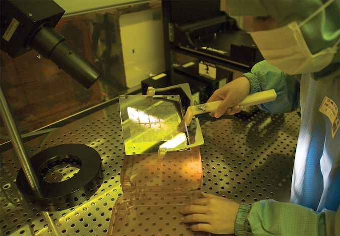
TSMC has revealed some additional details about its upcoming N2 and N2P process technology at its European Technology Symposium 2023. Both production nodes are being developed with high-performance computing (HPC) in mind, so, they feature a number of enhancements designed specifically to improve performance. Meanwhile, given the performance-efficiency focus that most chips aim to improve upon, low-power applications will also take advantage of TSMC's N2 nodes as they will naturally improve performance-per-watt compared to predecessors.
"N2 is a great fit for the energy efficient computing paradigm that we are in today," said Yujun Li, TSMC's director of business development who is in charge of the foundry's High Performance Computing Business Division, at the company's European Technology Symposium 2023. "The speed and power advantages of N2 over N3 over the entire voltage supply ranges as shown is very consistent, making it suitable for both low-power and high-performance applications at the same time."
TSMC's N2 manufacturing node — the foundry's first production nodes to use nanosheet gate-all-around (GAAFET) transistors — promises to increase transistor performance by 10-15% at the same power and complexity, or lower power usage by 25-30% at the same clock speed and transistor count. Power delivery is one of the corner stones when it comes to improving transistor performance and TSMC's N2 and N2P manufacturing processes introduce several interconnects-related innovations to squeeze some additional performance. Furthermore, N2P brings in backside power rail to optimize power delivery and die area.
Fighting Resistance
One of the innovations that N2 brings to the table is super-high-performance metal-insulator-metal (SHPMIM) capacitor to enhance power supply stability and facilitate on-chip decoupling. TSMC says that the new SHPMIM capacitor offers over 2X higher capacity density compared to its super-high-density metal-insulator-metal (SHDMIM) capacitor introduced several years ago for HPC (which increased capacitance by 4X when compared to previous-generation HDMIM). The new SHPMIM also reduces Rs sheet resistance (Ohm/square) by 50% compared to SHDMIM as well as Rc via resistance by 50% compared to SHDMIM.
Yet another way to reduce resistance in the power delivery network has been to rearchitect the redistribution layer (RDL). Starting from its N2 process technology, TSMC will use a copper RDL instead of today's aluminum RDL. A copper RDL will provide a similar RDL pitch, but will reduce sheet resistance by 30% as well as cut down via resistance by 60%.
Both SHPMIM and Cu RDL are parts of TSMC's N2 technology that is projected to be used for high volume manufacturing (HVM) in the second half 2025 (presumably very late in 2025).
Decoupling Power and I/O Wiring
The use of a backside power delivery network (PDN) is a yet another major improvement that will be featured by N2P. General advantages of backside power rail are well known: by separating I/O and power wiring by moving power rails to the back, it is possible to make power wires thicker and therefore reduce via resistances in the back-end-of-line (BEOL), which promises to improve performance and cut down power consumption. Also, decoupling I/O and power wires allows to shrink logic area, which means lower costs.
At its Technology Symposium 2023 the company revealed that backside PDN of its N2P will enable 10% to 12% higher performance by reducing IR droop and improving signaling, as well as reducing the logic area by 10% to 15%. Now, of course, such advantages will be more obvious in high-performance CPUs and GPUs that have dense power delivery network and therefore moving it to the back makes a great sense for them.
Backside PDN is a part of TSMC's N2P fabrication technology that will enter HVM in late 2026 or early 2027.


15 Comments
View All Comments
James5mith - Thursday, June 1, 2023 - link
"N2 is a great fit for the energy efficient computing paradigm that we are in today,"Hahahahahahahahahahahahahahahahahahahahahahaha
Energy efficiency has gone completely out the window these days. Core i5's need 150w of cooling now, and don't have much better performance than the old 65w variants from a few years ago.
m53 - Friday, June 2, 2023 - link
"TSMC's N2P fabrication technology that will enter HVM in late 2026 or early 2027"That is a minimum 2 year after intel introduces it with 20A and 18A. So it looks like Intel is really taking their manufacturing crown back. Of course it depends on whether Intel can really bring 20A by the end of 2024. But the recent comment from Nvidia CEO suggest they might.
my_wing - Wednesday, June 14, 2023 - link
TSMC N2P Backside is not equal to Intel PowerVia (20A). If Intel 20A is there by end of 2024 with GAA and PowerVia in place. Intel 20A > TSMC N2P in performance and density.If you look at the Intel slide, and this article just use the term to confirm my thinking "Backside Power Rail" (without mention nTSV), that TSMC N2P is 1st Gen Backside Power Delivery while PowerVia is 2nd Gen Backside Power Delivery, the Intel Paper shown PowerVia is Backside Power Rail + nTSV.
Basically, you see this way (think you are having a sandwich) .... M1(logic), M0, M1(power) ....; Backside Power Rail is that the copper wire goes through M1(power) to M0 to M1 (Logic) then like traditionally, the power still goes to logic side; PowerVia supplier the power from the back directly through the nTSV. TSMC like to take small steps at a time. So if Intel 20A delivery what is it then Intel is at least 1 full node ahead, just like the old days, it can be good or bad as intel has a history of milking the cow (toothpaste style again).
Oxford Guy - Sunday, June 4, 2023 - link
How many nanometers is '2nm'?my_wing - Wednesday, June 14, 2023 - link
7nm is N3 class.Then if you are asking why intel used ++++
TSMC N2 is 7nm++++++++++++++++++