TSMC Readies Five 3nm Process Technologies, Adds FinFlex For Design Flexibility
by Anton Shilov on June 16, 2022 3:10 PM EST
Taiwan Semiconductor Manufacturing Co. on Thursday kicked off its 2022 TSMC Technology Symposium, where the company traditionally shares it process technology roadmaps as well as its future expansion plans. One of the key things that TSMC is announcing today are its leading-edge nodes that belong to its N3 (3 nm class) and N2 (2nm class) families that will be used to make advanced CPUs, GPUs, and SoCs in the coming years.
N3: Five Nodes Over Next Three Years
As fabrication processes get more complex, their pathfinding, research, and development times get stretched out as well, so we no longer see a brand-new node emerging every two years from TSMC and other foundries. With N3, TSMC's new node introduction cadence is going to expand to around 2.5 years, whereas with N2, it will stretch to around three years.
This means that TSMC will need to offer enhanced versions of N3 in order to meet the needs of its customers who are still looking for a performance per watt improvement as well as transistor density bump every year or so. Another reason why TSMC and its customers need multiple versions of N3 is because the foundry's N2 relies on all-new gate-all-around field-effect transistors (GAA FETs) implemented using nanosheets, which is expected to come with higher costs, new design methodologies, new IP, and many other changes. While developers of bleeding-edge chips will be quick to jump to N2, many of TSMC's more rank & file customers will stick to various N3 technologies for years to come.
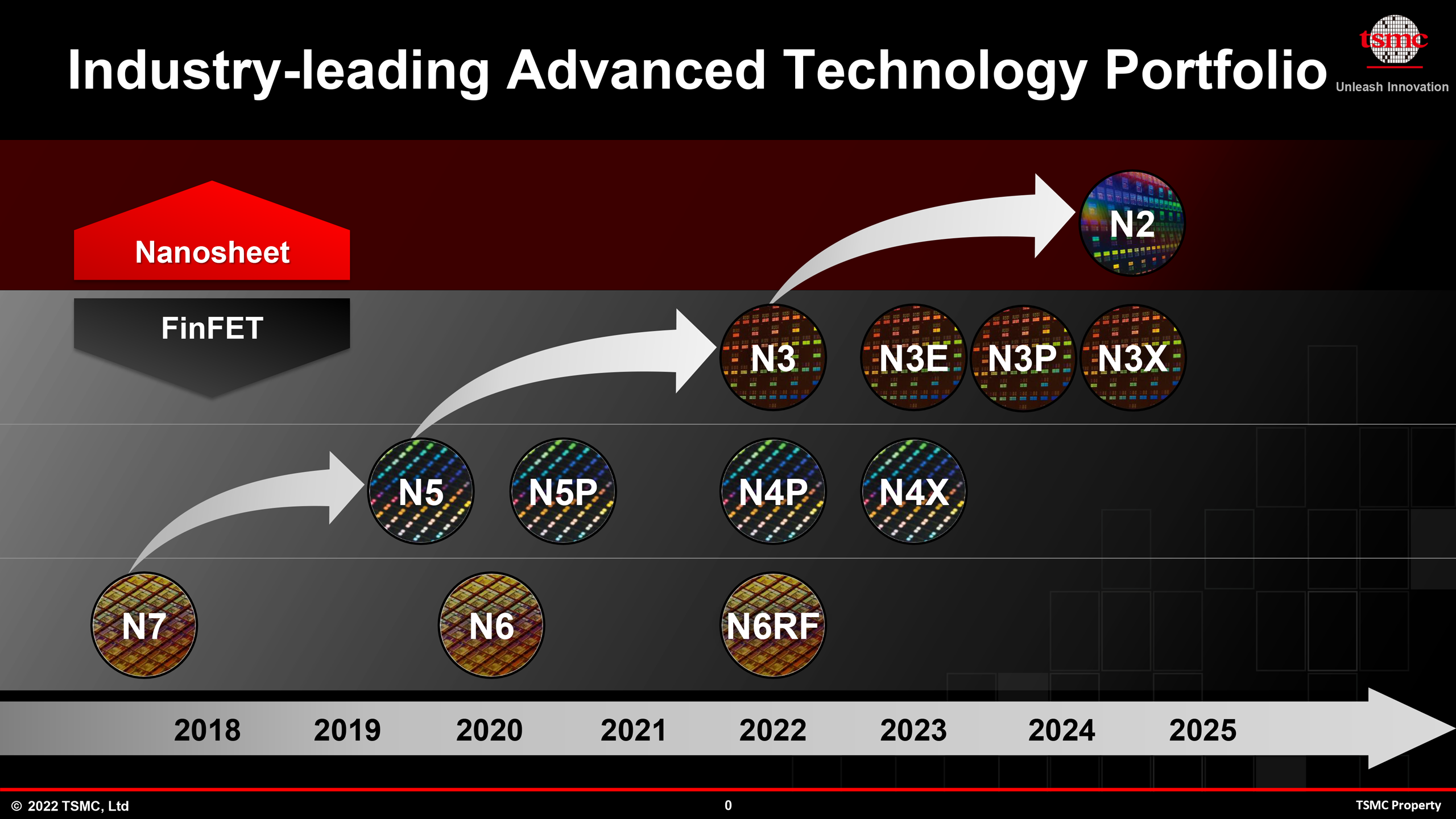
At its TSMC Technology Symposium 2022, the foundry talked about four N3-derived fabrication processes (for a total of five 3 nm-class nodes) — N3E, N3P, N3S, and N3X — set to be introduced over the coming years. These N3 variants are slated to deliver improved process windows, higher performance, increased transistor densities, and augmented voltages for ultra-high-performance applications. All these technologies will support FinFlex, a TSMC "secret sauce" feature that greatly enhances their design flexibility and allows chip designers to precisely optimize performance, power consumption, and costs.
| Advertised PPA Improvements of New Process Technologies Data announced during conference calls, events, press briefings and press releases |
||||||||
| TSMC | ||||||||
| N4 vs N5 |
N4P vs N5 |
N4P vs N4 |
N4X vs N5 |
N4X vs N4P |
N3 vs N5 |
N3E vs N5 |
||
| Power | lower | -22% | - | ? | ? | -25-30% | -34% | |
| Performance | higher | +11% | +6% | +15% or more |
+4% or more |
+10-15% | +18% | |
| Logic Area Reduction* % Logic Density* |
0.94x -6% 1.06x |
0.94x -6% 1.06x |
- |
? |
? |
0.58x -42% 1.7x |
0.625x -37.5% 1.6x |
|
| Volume Manufacturing |
2022 | 2023 | H2 2022 | 2023 | 2023 | H2 2022 | Q2/Q3 2023 | |
*Note that TSMC only started to publish transistor density enhancements for analog, logic, and SRAM separately around 2020. Some of the numbers still reflect 'mixed' density consisting of 50% logic, 30% SRAM, and 20% analog.
N3 and N3E: On Track for HVM
TSMC's first 3 nm-class node is called N3 and this one is on track to start high volume manufacturing (HVM) in the second half of this year. Actual chips are set to be delivered to customers in early 2023.This technology is mostly aimed at early adopters (read: Apple and the like) who can invest in leading-edge designs and would benefit from the performance, power, area (PPA) advantages offered by leading-edge nodes. But as it's tailored for particular types of applications, N3 has a relatively narrow process window (a range of parameters that produce a defined result), which may not be suitable for all applications in terms of yields.
This is when N3E comes into play. The new technology enhances performance, lowers power, and increases the process window, which results in higher yields. But the trade-off is that the node features a slightly reduced logic density. When compared to N5, N3E will offer a 34% reduction in power consumption (at the same speed and complexity) or an 18% performance improvement (at the same power and complexity), and will increase logic transistor density by 1.6x.
It is noteworthy that, based on data from TSMC, N3E will offer higher clockspeeds than even N4X (due in 2023). However the latter will also support ultra-high drive currents and voltages of above 1.2V, at which point it will be able to offer unbeatable performance, but with very high power consumption.
In general, N3E looks to be a more versatile node than N3, which is why it is not surprising that TSMC has more '3nm tape outs' at this point than it had with its 5 nm-class node at a similar point of its development.
Risk production of chips using N3E is set to start in the coming weeks (i.e., in Q2 or Q3 2022) with HVM set for mid-2023 (again, TSMC does not disclose whether we are talking about Q2 or Q3). So expect commercial N3E chips to be available in late 2023 or early 2024.
N3P, N3S, and N3X: Performance, Density, Voltages
N3's improvements do not stop with N3E. TSMC is set to bring out N3P, a performance-enhanced version of its fabrication process, as well as N3S, density-enhancing flavor of this node, some time around 2024. Unfortunately, TSMC is not currently disclosing what improvements these variants will offer compared to baseline N3. In fact, at its Technology Symposium 2022, TSMC did not even show N3S in its roadmap and it only got mentioned by Kevin Zhang in a conversation. Bearing all this in mind, it is really not a good business to try guessing characteristics of N3S.
Finally, for those customers who need ultra-high performance no matter power consumption and costs, TSMC will offer N3X, which is essentially an ideological successor of N4X. Again, TSMC is not revealing details about this node other than that it will support high drive currents and voltages. We might speculate that N4X could use backside power delivery, but since we are talking about a FinFET-based node and TSMC only going to implement backside power rail in nanosheet-based N2, we are not sure this is the case. Nonetheless, TSMC probably has a number of aces up its sleeve when it comes to voltage increases and performance enhancements.
FinFlex: N3's Secret Sauce
Speaking of enhancements, we should definitely mention TSMC's secret sauce for N3: FinFlex technology. In short, FinFlex allows chip designers to precisely tailor their building blocks for higher performance, higher density, and lower power.
Update 6/17: The initial version of the story incorrectly referred standard cells and blocks as transistors, which has been corrected.
When using a FinFET-based node, chip designers can choose between different libraries using different standard cells. A standard cell is the most basic building block that performs a Boolean logic or storage function and consists of a group of transistors and interconnects. From math point of view, the same function can be performed (with the same result) using a standard cell of different configurations. But from manufacturability and operation point of view, different standard cell configurations are characterized by different performance, power consumption, and area. When developers need to minimize die size and save power at the cost of performance, they use small standard cells. But when they need to maximize performance at the trade-off of die size and higher power, they use large standard cells.
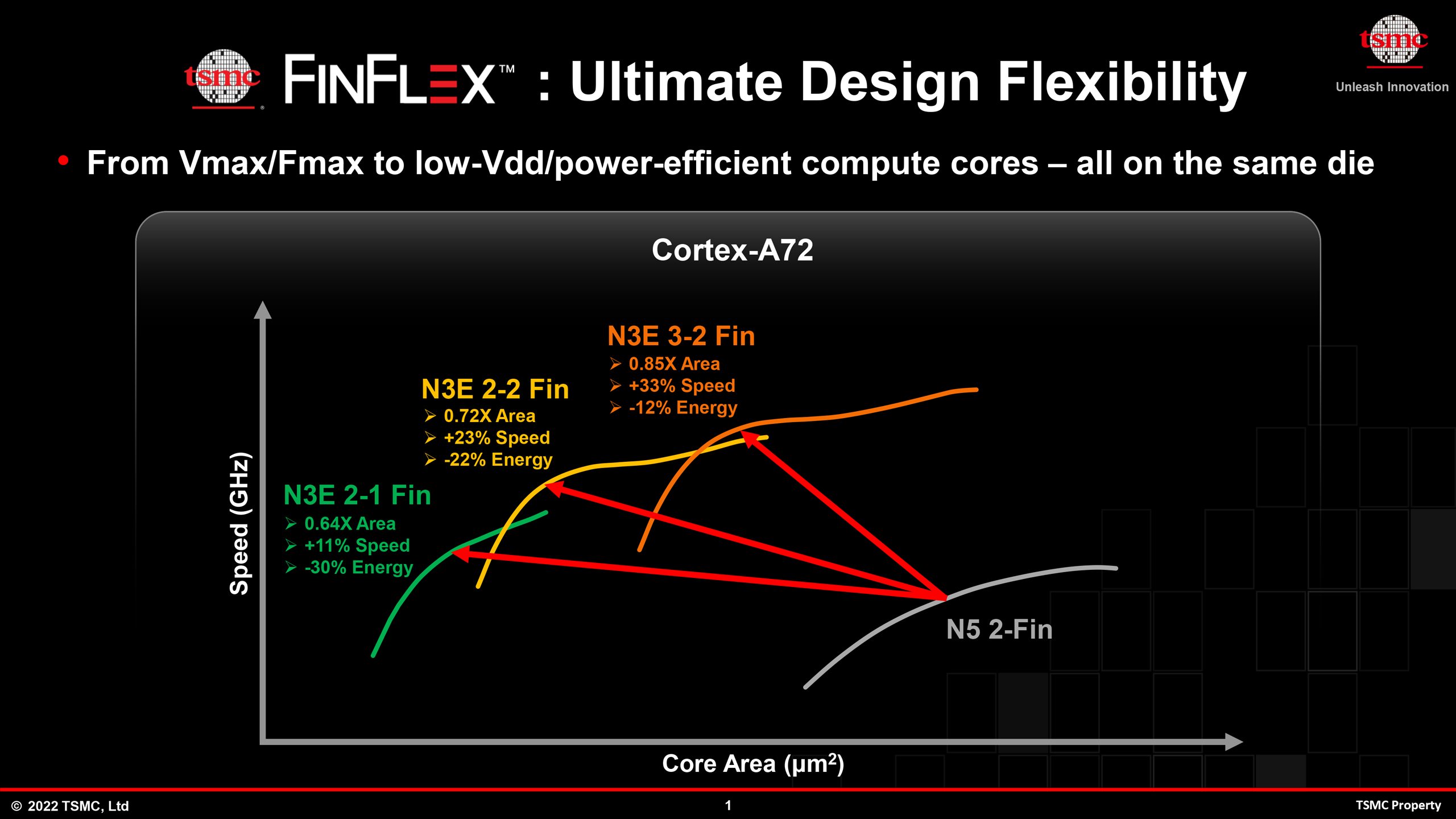
Currently, chip designers have to stick to one library/standard cells either for the whole chip or the whole block in a SoC design. For example, CPU cores can be implemented using 3-2 fin blocks to make them run faster, or 2-1 fin standard cells to reduce their power consumption and footprint. This is a fair tradeoff, but it's not ideal for all cases, especially when we are talking about 3 nm-class nodes that will be more expensive to use than existing technologies.
For N3, TSMC's FinFlex technology will allow chip designers to mix and match different kinds of standard cells within one block to precisely tailor performance, power consumption, and area. For complex structures like CPU cores, such optimizations give a lot of opportunities to increase core performance while still optimizing die sizes. So, we are eager to see how SoC designers will be able to take advantage of FinFlex in the looming N3 era.
FinFlex is not a substitute for node specialization (performance, density, voltages) as process technologies have greater differences than the ibraries or transistor structures within a single process technology, but FinFlex looks to be a good way to optimize performance, power, and costs for TSMC's N3 node. Ultimately, this technology will bring the flexibility of FinFET-based nodes a little closer to that of nanosheet/GAAFET-based nodes, which are slated to offer adjustable channel widths to get higher performance or reduce power consumption.
Summary
Like TSMC's N7 and N5, N3 will be another family of long-lasting nodes for the world's largest contrast maker of semiconductors. Especially with the jump to nanosheet-based GAAFETs coming up at 2nm for TSMC, the 3nm family will be the final family of "classic" leading-edge FinFET nodes from the firm, and one that a lot of customers will stick to for several years (or more). Which, in turn, is why TSMC is prepping multiple versions of N3 tailored for different applications – as well as FinFlex technology to give chip designers some additional flexibility with their designs.
The first N3 chips are set to enter production in the coming months and arrive to the market in early 2023. Meanwhile, TSMC will keep producing semiconductors using its N3 nodes long after it introduces its N2 process technology in 2025.


43 Comments
View All Comments
Bruzzone - Friday, June 17, 2022 - link
TouchdoenTom9, Have you considered Intel 'fast follower' does not want the node lead on observing and learning and well, doing what Intel does keeping tabs on TSMC. Intel itself buffered into TSMC between 6 nm and 3 nm to monitor its own in-house progress v Intel designs at TSMC. Here's the economic reason for fast follower. As long as Intel trails TSMC by one node Intel is always on the downward sloping (depreciating) cost curve of the prior or lagging node as TSMC moves to the upward sloping cost curve of every next leading node. On this technique Intel cost is always going down as TSMC cost is going up. Think opposing low high sign wave. On leading, Intel's best chance to leap frog is advanced packaging and Intel would like to sell TSMC back end packaging between Chandler and Rio Rancho? I think so. mbKAlmquist - Friday, June 17, 2022 - link
Intel's failure to maintain the lead in process technology was not intentional. They are currently behind because of execution failures, not because they planned to fall behind. If they successfully execute on their current road map (which, as techjunkie123 says, is quite aggressive), they may well regain the lead.The economic benefits of being a fast follower are questionable. The “depreciating cost curve” is an accounting convention. Building a new fab (or upgrading an existing fab to use a new process) is an expensive proposition, and the money needs to be shelled out up front, before the fab generates any revenue. The accountants will amortize this cost over the expected life of the fab. The accountants expect the prices customers are willing to pay to drop over time as more fabs are built that support a similar or more advanced process. Therefore, they will allocate more of the cost of building the fab to chips manufactured early in the life of the fab, and less of the cost to chips manufactured later on.
What that means is that, if you build a fab, the cost of manufacturing a chip reported by the accountants will decrease over time. It does not mean that you can lower your costs simply by bringing a fab on line later. To decrease your costs, you actually have to decrease the cost of building the fab. Lagging behind your competitors does have the potential to decrease costs, both because there is the possibility that equipment manufactures will decrease their prices, and because competitors may reveal helpful information. I doubt that either of these are enough to make up for the opportunity cost of not being able to sell cutting edge products. There are large markets for processes that are well behind the state of the art, but being just marginally behind the state of the art means you are competing directly with people who are at the state of the art.
tyb60 - Friday, June 17, 2022 - link
Well said, and why their current strategy requires tens of billions of tax payer money as the model is flawed from the beginningkwohlt - Sunday, June 19, 2022 - link
Just pointing out that both Samsung and TSMC are heavily subsidizedBruzzone - Thursday, June 23, 2022 - link
KAlmquist,"Intel's failure to maintain the lead in process technology was not intentional. Execution Failure".
Hum? How about sabotage in a multipoint manipulation by internal and external gangs is my take on 1) industry actors taking law enforcement subject monopoly regulation into their own hands disgusted by 30 years of nonregulation, and 2) parallels $350 billion DCG hard cost loss associated Xeon product laundering theft would have paid for a lot of R&D and PC&E.
The economic benefits of fast follower I concur a short run benefit, technique, in relation long run cost : price / margin recovery of Capital Expenditure associated Plant, Construction, Equipment.
By simply cost optimizing Intel can return up to $23 billion a year to the bottom line. CFO Zinser has set a 30% cost reduction objective associated avoidable and unnecessary expenditure here are three from my view; 1) sales close incentive aka bundle deal freebie, 2) unnecessary soft marketing expenditures, 3) avoidable financial leaks and I'll be direct here; employees in cahoots with customer gang thefts.
By Intel closing its financial leaks, minimally + 30% revenue per year can be redirected to research, development, plant, construction and equipment and maintenance.
These are Intel's basic cost centers in 2021 on production of 391,800,000 components of all types; 221,800,00 Core products that is Gartner annual PC less my AMD all up at 118 M. In additional on my Intel data 70 M Xeon which into 2022 has currently halved. Plus 100 M control hubs, NICs, SSD memory controllers, possibly Atom supply sows a dead product line that Intel contracts to foundries.
If Intel sell for $39 or less contracted out and at $79 still within variable cost range is cost effective to contract out.
In 2021 average total cost = $306.76 per unit and to make a 55% gross margin Intel needs to charge $475.47 to OEM where $1K price would be $713.20 at x1.5 margin.
Intel needs to raise price by 135% and if Sapphire Rapids as a Xeon price support does that Intel will be in good shape. But if not and Sapphire Rapids stalls into q3, Intel declaring Chapter 11 isn't off the table and is among the options of any structural reconfiguration.
I don't believe SR is delated by the way solely hardware ahead of software specific what is whole (mass market) product beyond business of compute as a self sufficient whole platform developer.
Now let's consider PC&E cost is $63,245,000,000 in 2021, Intel depreciates physical infrastructure between 20 and 30 years and equipment over seven years which is two to two plus one-half process cycles and I think Intel 7, 4(5), 3, 2.8 and 1.8 is not five but 2.5 traditional lithography cycles, tick tock on the stretch of the lithography equipment. However, if it is not 2.5 cycles and ends up being 5 cycles that's costly and Intel isn't talking about the additional cost of advanced packaging.
Rocks Law doubles cost every process node to double transistors and let's keep that in mind, it's relevant but not in the way it once was, although, advanced packaging is costly and over the short run likely exceeds dice fabrication cost.
On PC&C brown and greenfield Intel plans to invest between Arizona build, Rio Rancho retrofit, Hillsboro retrofit, Leixlip retrofit, Ohio build and Europe build a total of $229,500,000,000.
Minimally straight lined out over 20 years the capital expenditure adds $21.354 billion per year through 2027 then drops to $12.8 billion in maintenance. This is obviously a simple way of looking at the impact of capital investment.
In 2021 PC&E increased on average 2% per quarter with q4 2021 up 11.7% from q4 2020. If Intel proceeds with all projects suggested, PC&E will increase from $63.245 billion to $84.6 billion and despite depreciation that cost never truly goes down for every depreciation credit debited to sustained maintenance.
At PC&E $84.6 billion, per unit cost charge gains from $161.41 to $214.83 and ATC is now $360.16 + 17.4% on the same unit volume as 2021 = 391.8 M where the idea is to produce more product maintaining efficiency of the manufacturing cost structure. Intel would have to increase production 33% to 521 M units to maintain PC&E at $161. 2020 I have Intel production at 500 M units that was mostly 14 nm run end.
On price situation 2021 is up over 2020 by 29.5% per unit at $155.73 to $201.69 and gross up $87.22 to $111.83 respectively Intel was in bad shape and no wonder Intel had to retool as DCG and Core lines hit variable cost hard in 2019 and 2020 respectively.
At 521 M units Intel annual revenue is $105 billion at constant $201.69 per unit but that price could increase dependent performance and competitive situation.
I expect on Rocks Law not a doubling, however PC&E cost line will approach $100 billion by the time Intel reaches 2.8A at which time PC&E per unit at 2021 volume will be $255.23 and ATC $400.57. To maintain PC&E at $161 per unit Intel will need to sell 620 M units for revenue value $125 billion and that's within 5 years.
That's a revenue increase at constant $201 per unit and fixed plus variable cost which will go up on manpower requirement by 58%. R&D will also increase and I'm not taking into account variable and R&D increases in these estimates.
To maintain the competitive price of $201.69 Intel top shelf margin will have to cover it as it does today and where down bin components represent a gross margin drag. By the time Intel PC&E doubles from 2022 at $84 billion to $168 billion per unit cost at the 2021 constant is $429 and to keep PC&E constant at $161 Intel will have to sell 1 billion units valued $209 billion. Intel is both an IDM and foundry by this time and Intel foundry will not be producing low priced components on the margin requirement. Legacy will be prior four to six process nodes and these will be premium products primarily.
In summary if Sapphire Rapids or any other Xeon for the needed price support fails or is rejected by the customer base, Intel declares bankruptcy remains one of the options.
If things take a turn for the worst in the next two years during fab construction, intuitively its the classic Intel to misrepresent the situation leading up to a failure and Intel will land themselves in Chapter 11, And on any partial fab construction site sitting their Intel would ask the government to assist in the completion of the project.
This is classic Intel reversing the obvious on some high hurdles to reconfigure the business from its nonorganic extra economic monopoly cost structure that is extraordinary impacted on the cost of corporate theft. Intel should already have these fabs developments built, productive and paid for.
Mike Bruzzone, Camp Marketing.
tyb60 - Friday, June 17, 2022 - link
Intel has publicly said they aspire for leadership and not to be a fast follower, go research Pat's ambitions!They claim the IDM+Foundry is a competitive advantage. It is actually a flawed thinking as when you are an IDM your first priority is to fab your own designs in your own factory for advantage. All your competitors won't use you. Those that don't compete will always wonder and rightly so whether you prioritize your own internal designs over theirs. Foundry by definition is agnostic, not really, but they don't compete against their customers.
Running a trailing node as Intel is with 10nm and their intel 7 which really is 10 nm makes their internal products bigger, more power hunger and costlier than AMD, Nvidia, Apple and everyone else that has access to Foundry 5nm, 4nm and soon 3nm. Also they have the ability to leverage the foundry scale which means cheaper because bigger volume than Intel.
Your concept of depreciation is flawed. Intel has to depreciate their new tools regardless of lagging node or new node. Actually you can see this in the financials as margins are plummeting as they now are depreciating their expensive 10nm fabs. Foundry with their scale can depreciate across a far larger volume and they continue to run their fabs for many years at pure profit after they are depreciated. As and IDM Intel has to flip its fabs to leading edge as they have nothing to fill their older fabs and why they now are trying desperately to get into the Foundry space.
If you think the IDM model is superior look at the GM for the past few years of Foundry and considering adding the GM of their customers and compare with the total GM of Intel to see who has the better business model.
You should check on package, I don't think Intel is that superior than what is offered to the likes of Apple and AMD from Foundry space
Turbofrog - Wednesday, June 22, 2022 - link
"Running a trailing node as Intel is with 10nm and their intel 7 which really is 10 nm makes their internal products bigger, more power hunger and costlier than AMD, Nvidia, Apple and everyone else"This isn't really accurate in terms of real world products. An Alder Lake i7-12700K is a monolithic 215 mm^2 square die. That's pretty close to the 206 mm^2 total die area of the Ryzen 5800X and substantially smaller than the 287 mm^2 die area of the 5900X.
That i7-12700K outperforms both Ryzen processors in both single-core and multi-core performance, and depending on the load (i.e. gaming) can even achieve superior performance per watt.
So it's clearly not accurate to characterize Intel 7 as "really a 10nm node" when it is competitive or superior to the TSMC N7 node that it is directly competing with today. Unless you want to argue that TSMC N7 is also "really a 10nm node." I guess that's fine, but an unnecessary semantic debate...
Bruzzone - Friday, June 17, 2022 - link
TdT9, Interesting point on Intel process and product road map alignment. mba668g - Monday, June 20, 2022 - link
I even have made $45,030 just in five weeks straightforwardly working part-time from my apartment. (tec-21) Immediately when I've lost my last business, I was exhausted and luckily I found this top online task & with this I am in a position to obtain thousands directly through my home. Everybody is able to get this best career & can gain more dollars on-line going this article.http://jmlebbe.free.fr/cours/courses/MPOGG/documen...
a668g - Monday, June 20, 2022 - link
I even have made $45,030 just in five weeks straightforwardly working part-time from my apartment. (tec-21) Immediately when I've lost my last business, I was exhausted and luckily I found this top online task & with this I am in a position to obtain thousands directly through my home. Everybody is able to get this best career & can gain more dollars on-line going this article.http://comproject.free.fr/courses/TOWERKLUB_001/do...